
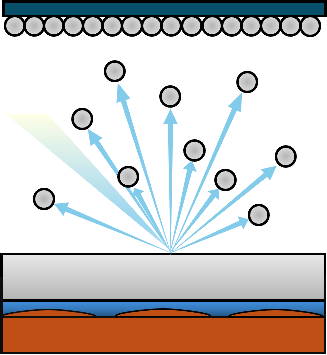
Plasma Vapor Deposition (PVD) is a technique used for applying thin coatings on applications such as door knobs, drill bits, and decorative plating on phones and watches. The target material that creates the coating is connected to a conductive backing plate by a bonding layer. In order to deposit and sputter the material to create a film, the target material is heated in an electric field to move atoms of the target onto the desired material. Because heating makes it easier to remove atoms from the target material, the deposition rate is therefore limited by the melting temperature of each layer. Indium is traditionally used as a bonding layer, and compared to the other layers has the lowest melting temperature of 156°C.
To improve upon the current bonding layer and ultimately decrease the processing time of PVD, a new alloy must maintain the thermal conductivity and softness of Indium, while simultaneously increasing the melting temperature. This project investigates a new alloy composition to meet these requirements, resulting in faster processing speeds and greater efficiency with PVD systems, and therefore more throughput for PVD thin films and coatings.